[ad_1]
Eighty cores is twice the amount you can currently purchase from Intel for up to $8,099, though it’s only a third more than what AMD could sell you for $7,890. But Intel’s flashiest Xeons and AMD’s shiniest Epycs are more similar than you’d imagine; they share the same clock speeds, the same memory options, and the same TDPs. AMD has an upper hand in PCIe connectivity, but Intel’s got better on-chip connectivity, etc.
Sapphire Rapids, Intel’s fourth-generation Xeons, share more emerging technologies with GPUs than with other CPUs. Nvidia’s five-figure A100, for example, is the only GPU to offer up to 80 GB of HBM2e memory. Sapphire Rapids has 64 GB of HBM2e onboard (and eight lanes of DDR5 memory, too). The A100 was the first GPU to support BF16 computation. Sapphire Rapids will support BF16, too.
Sapphire Rapids also has PCIe 5.0, a new core architecture called Willow Cove, the 10nm Enhanced SuperFin node, and the new LGA4677-X socket on its resume.
All this is public information that Intel has divulged, mostly intentionally. Intel had begun sampling Sapphire Rapids to partners by the end of last year, Intel’s now-former CEO Bob Swan said to investors in January. Multiple sources have said that the sample models had 28 cores enabled.


The story takes a violent turn
At the end of January, a regular leaker on the Chinese site Bilibili gained ownership over one of the disseminated samples. He took some photos, then delidded the processor in the most awful way possible. Twenty seconds into this clip, he puts the processor in a regular bench vice and just starts cranking. Before the minute mark, he’s heating it over a gas stovetop flame, and then – brace yourself – he accidentally drops the processor into the flame. (If you’re curious, an oven is usually considered best practice, partly to avoid this issue.)
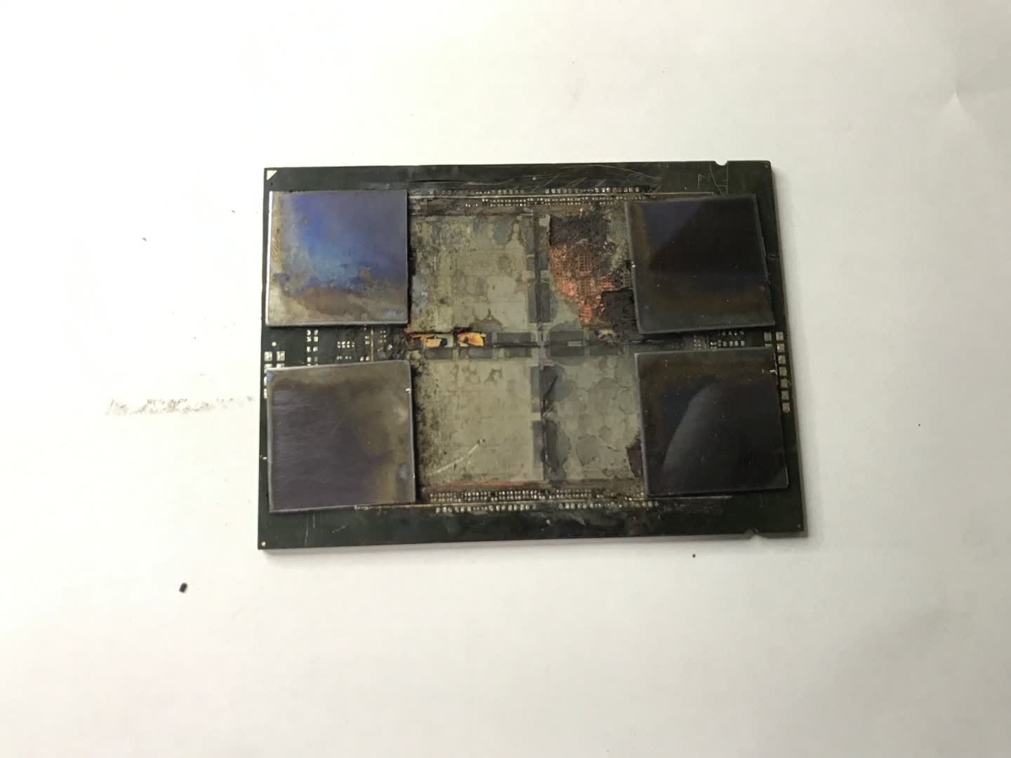
Afterward, the heat spreader comes off quite easily. An autopsy reveals that the heat spreader was soldered to the die using indium, like Rocket Lake.
Under the heat spreader was a quad-chiplet formation. It’s theorized, but not with much certainty, that Intel is using EMIB (embedded multi-die interconnect bridge) or Foveros to connect the chiplets and the HBM2e memory to gain an inter-chip bandwidth advantage over AMD’s Infinity Fabric.

Leaker commits an atrocity
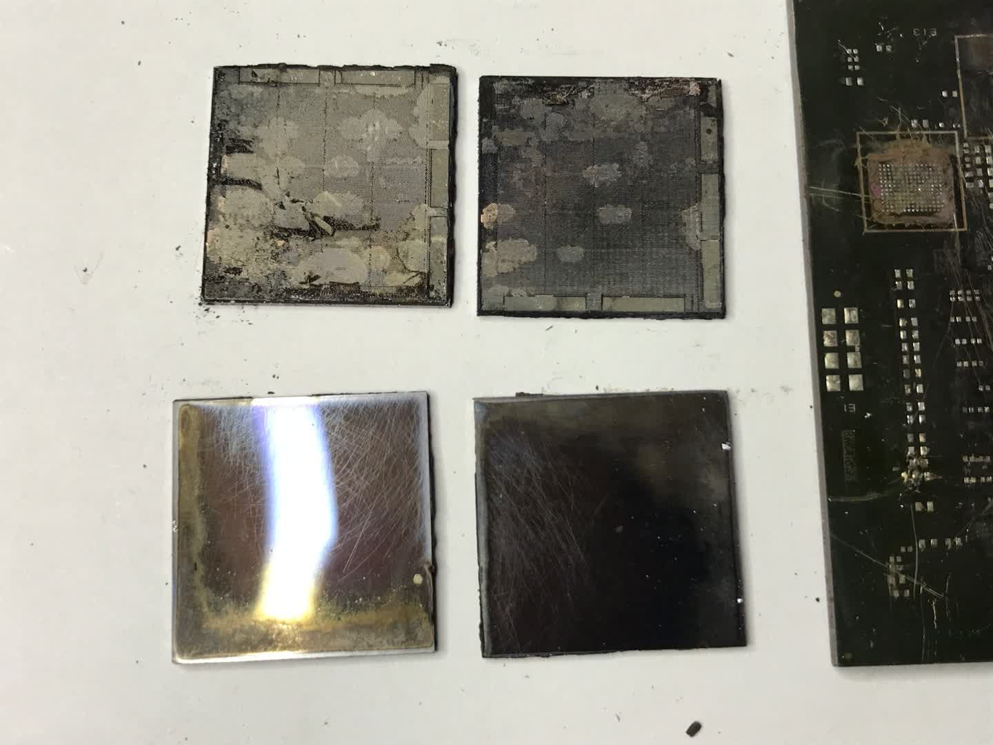
Last week, the leaker pulled all four of the chiplets off the substrate, then dissected them. It appears as if he successfully removed the HBM2e chips from three of the chiplets. The fourth… it’s best not to look.
Removing the HBM2e chips revealed the cores underneath. From the looks of it, each chiplet contains twenty cores arranged in a five by four grid. There also seem to be several controllers and possibly interconnect arrays around the perimeter of each chiplet.
The twenty cores took the leaker by surprise. It had been leaked, repeatedly, that Sapphire Rapids would top out at 56 cores. If that were the case, then Intel would be disabling six of the twenty cores on each chiplet, a proportion unprecedented in a flagship model. It’s possible that the 56-core leaks were simply wrong, and it’s also possible that not all of the arrangements that look like cores are in fact cores. The most depressing possibility is that Intel’s new node has an absurdly high failure rate.


Image credit: Michael Dziedzic, Yuuki_AnS
[ad_2]
Source link